A 100 MHz CPU implemented on the Virtex-5 FPGA with hardware graphics acceleration. Includes a three-stage pipeline, caching, UART, and a display monitor with fast drawing of lines and circles.
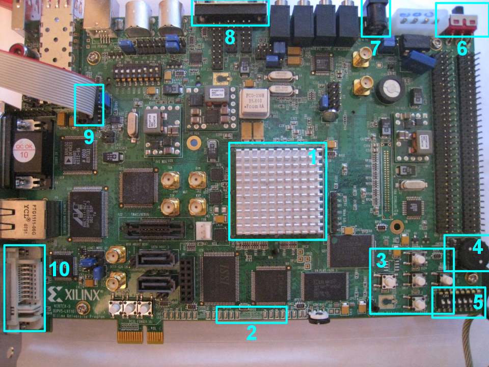


The CPU is fully functional with a three-stage pipeline implementing the RISC-V instruction set on the Virtex-5 FPGA (XUPV5-LX110T development board). It features memory-mapped IO for UART, direct pixel control of a monitor, and graphics acceleration for quickly drawing lines and circles. Two-way set associative write-back caches are used for both instructions and data. The graphics accelerator can draw lines and circles directly to the screen using the Bresenham’s line and Midpoint circle algorithms.
This was the final project for CS150—Components and Design Techniques for Digital Systems. For more details, read the project report below or download the PDF version.
CS150 Project Final Report
Team 1: Max Nuyens and Casey Duckering
Project Functional Description and Design Requirements
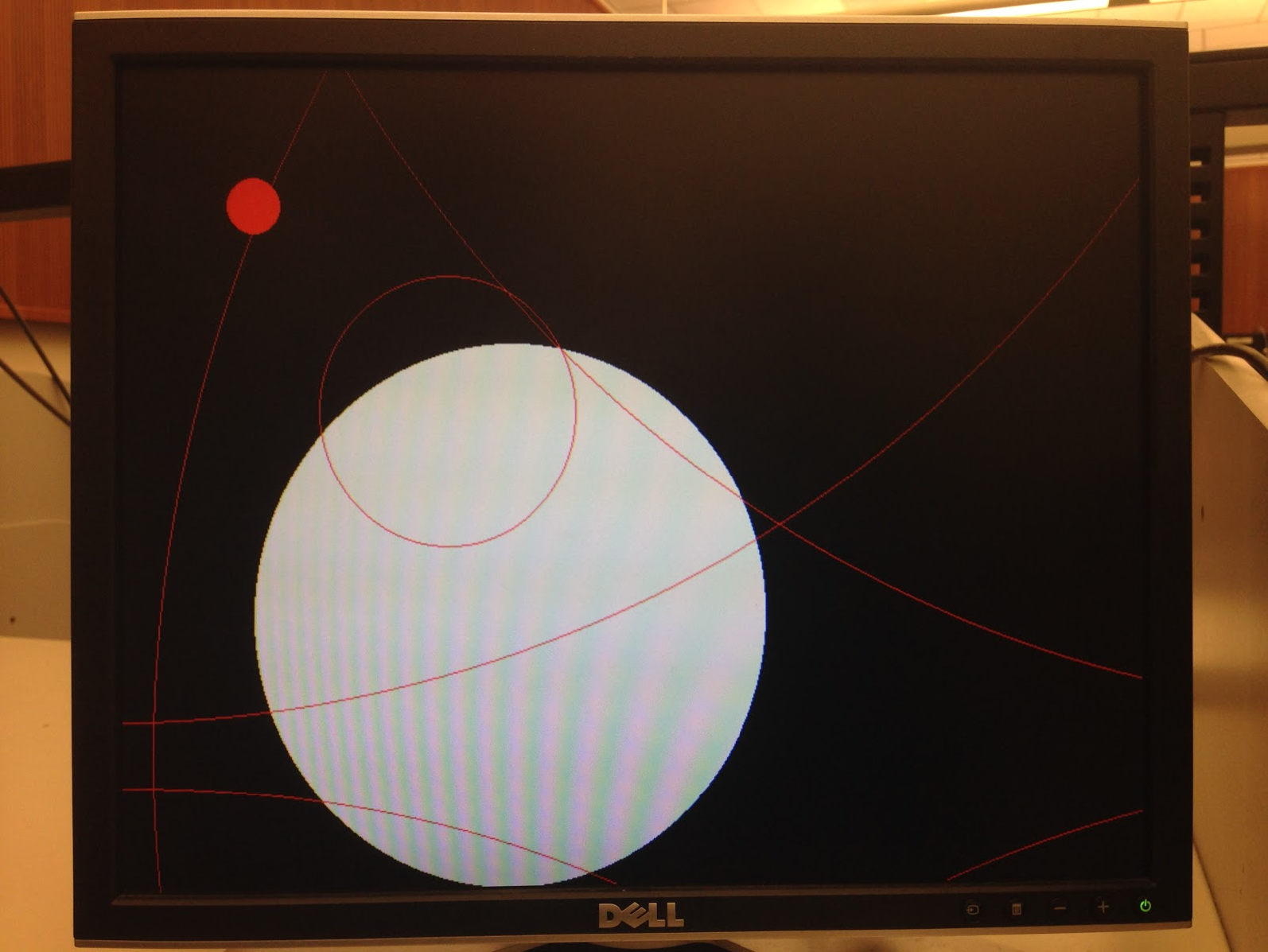
The objective of our project was to implement a functional three stage pipelined RISC-V CPU running 32-bit RISC-V instruction set at 100 Mhz, with two way set associative write-back instruction and data caching. The memory architecture was required to include a cache bypass and memory mapped IO for UART, cycle and instruction counters, and graphics acceleration. The graphics accelerator needed to have the capability to draw lines and fill a screen with a solid color. We expanded this feature to add the ability to draw circles, open and filled, on the screen. A sample image is attached (Appendix: Figure 3).
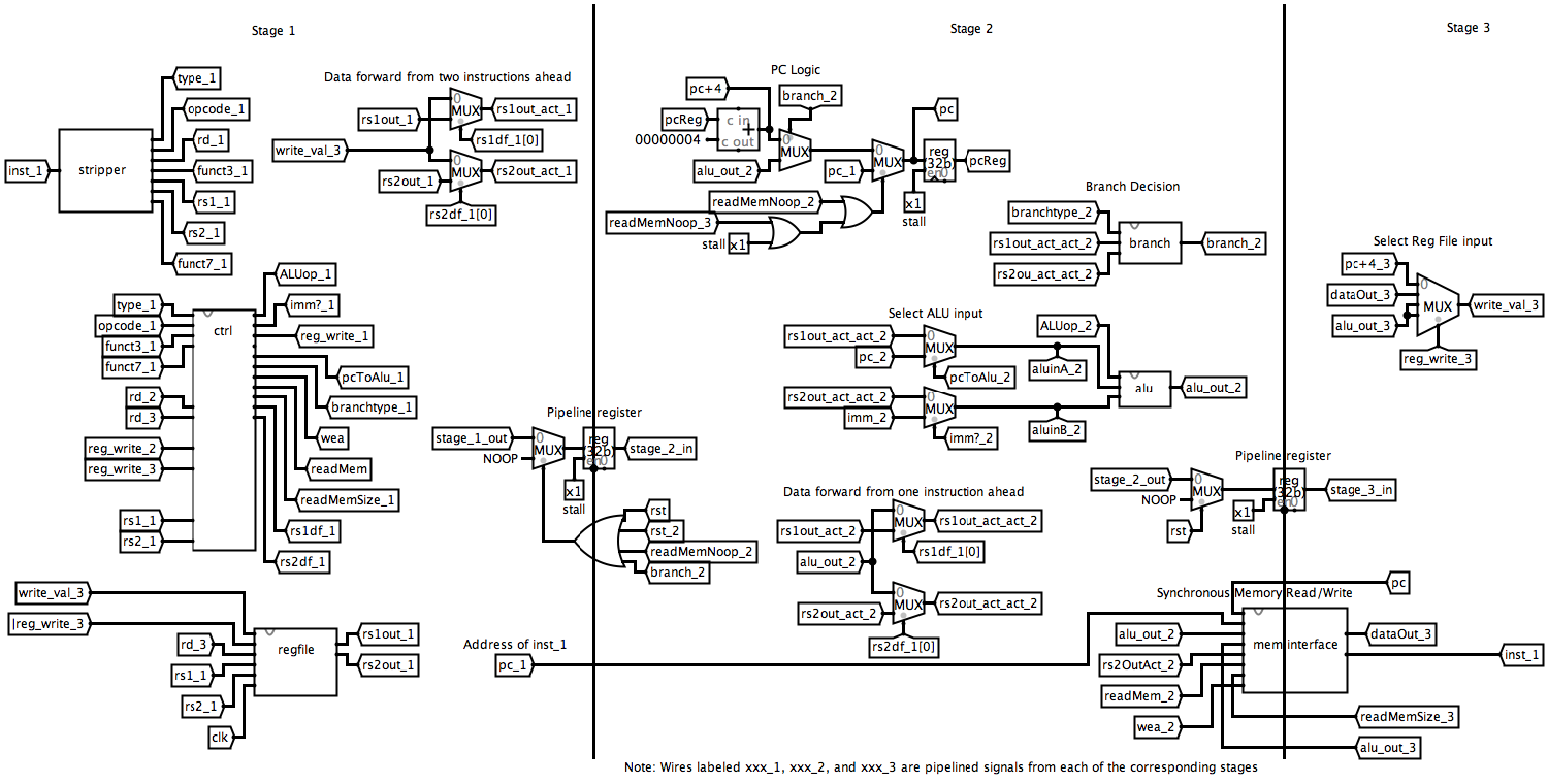
High-level organization
Our design is split up into three main stages. We’ve provided a block diagram of our data path (Appendix: Figure 2) as well as the following descriptions of each stage.
Stage 1
In stage one we receive the instruction from memory, analyze it, and generate control signals for the rest of the design. We also access the register file to get any necessary values, and handle data forwarding from stage 3 (two instructions away).
This uses the modules: Control, Stripper, ImmDecode, and RegFile.
Stage 2
In stage two we execute arithmetic with the ALU, handle branching (and jumping) logic, and input to the memory mapped IO. Data forwarding from the previous instruction is received from stage 3 at the beginning of this stage.
This uses the modules: MemoryInterface, ALU, and Branch.
Stage 3
In stage three, we receive the output from the memory or memory mapped IO and write to registers from either the ALU, memory, or the PC+4 according to the control signal. The data output of the stage is sent back to the first stage for data forwarding. If data forwarding from memory, a noop is inserted to reduce the critical path.
This uses the modules: MemoryInterface, and RegFile.
PC Logic
The PC is normally incremented by 4 every cycle. On a stall, the PC value is held the same and on reset, the PC is set to 0x40000000 (the start of BIOS memory). On branches, it is set to the address computed by the ALU and there is additional logic to stall the PC when noops are inserted when data forwarding from memory.
Detailed Description of Sub-pieces
Control
Takes in fields of the instruction from the Stripper and outputs all control signals based on only the current instruction except address based control signals used in MemoryInterface because the memory address isn’t known in the first stage.
Stripper
Takes in an instruction and splits it into fields for opcode, rs1, etc. for other modules to use. Also outputs the instruction type based on the opcode.
ImmDecode
Takes in the current instruction and instruction type, and decodes the immediate of the current instruction sign extended to 32 bits. The immediate is stored in different bits for the different instruction types R, I, S, SB, U, and UJ.
RegFile
Maintains the values of 32 32-bit registers. Stores values into a register synchronously and reads two values at a time asynchronously and always outputs zero for register zero.
ALU
Takes in two 32-bit inputs and an operation type and then computes the result.
Branch
Takes in two 32-bit values to compare, and the type of comparison to do (registered from Control) and outputs whether to branch or not. Always outputs true if the type is a jump.
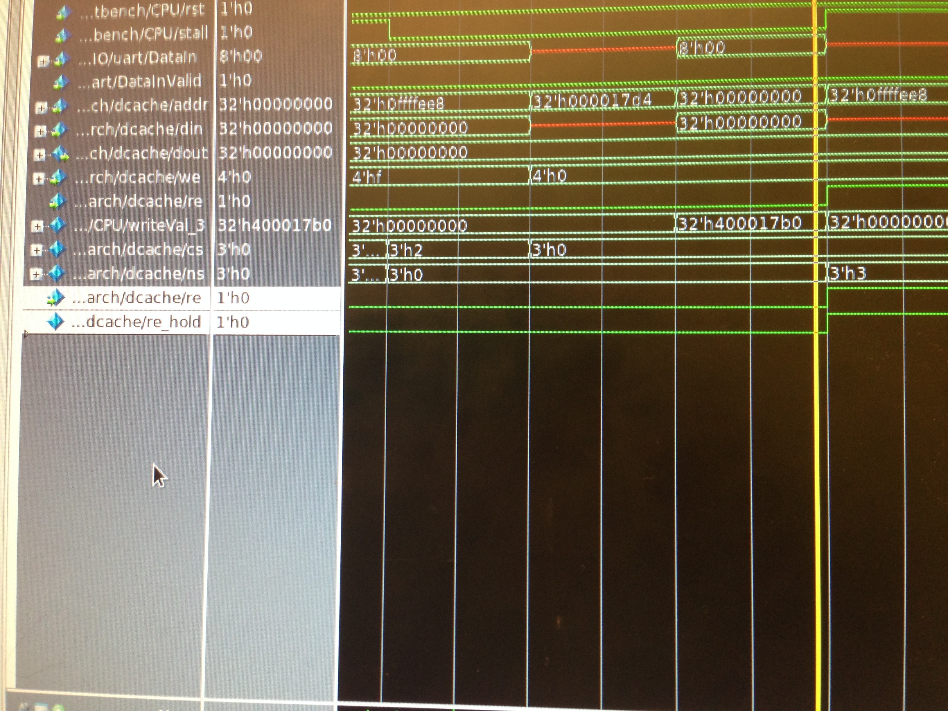
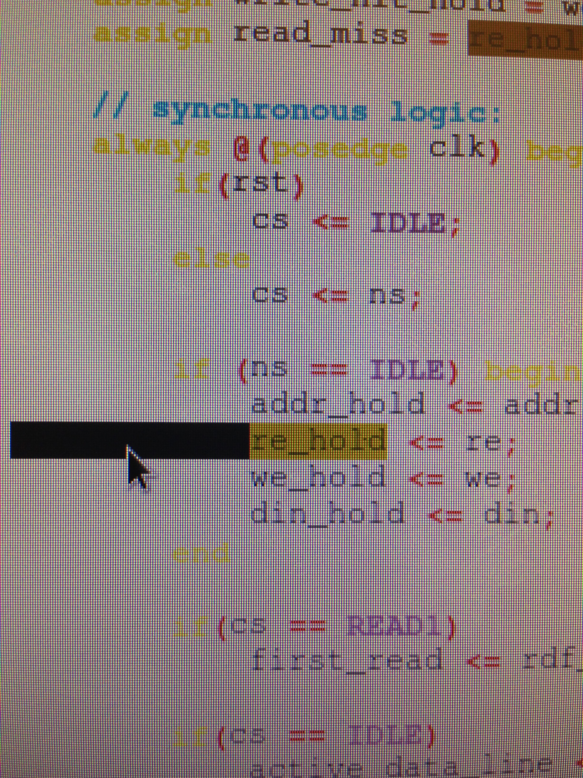
MemoryInterface
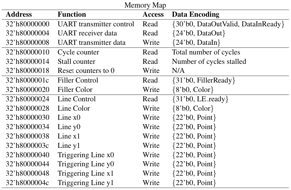
Takes in an address, and a read and write enable, and based on the top nibble of the address either accesses memory through different caches, or access peripherals of the cpu, based on the tables below.

MemoryInterface also takes in the PC and outputs instructions using the instruction cache. It holds the outputs of the caches if they output while anything else is stalling, so at the end of the stall, all values are ready.
Status and Results
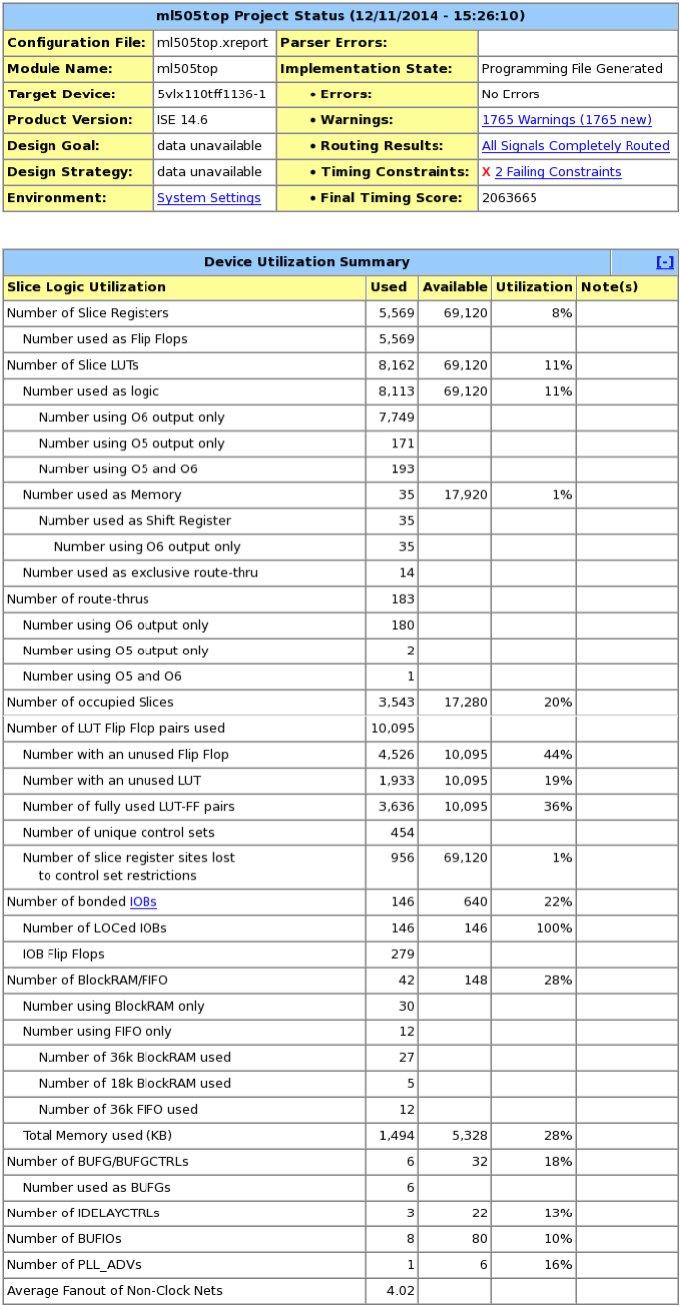
Everything (2 way set associative write back cache, graphics accelerator, all instructions in the spec, UART, counters, and cache bypass) works at 100 Mhz. We fail two timing constraints, but they don’t affect the ability of our cpu to run correctly at speed. We believe this is because the longest critical path is only used during a stall, so it actually has two cycles to stabilize.
Slice LUTs: 8162
LUT Flip Flop Pairs: 10095
For your convenience we’ve attached a copy of the report main screen (Appendix: Figure 1), in case we forgot any number you wished to see.
Conclusions
This project was a challenge, but as predicted, the challenge was mostly in debugging the mistakes we made rather than in writing the code in the first place. Hence most of the lessons we learned were about how to better debug Verilog and other similar languages. Bugs are very often in the connections between pieces as opposed in the individual modules, so it would have been better if we’d checked these connections carefully in the beginning of our debugging process as opposed to after a week or two. Verilog is very bad a throwing errors for typos, and we should have created something that would show us only the errors that we had caused.
Appendix